
Etched Comes out of Stealth, Again.
The Age of Inference, not innocence. Peter Thiel kids with backing from Jane Street and TSMC affiliated VC.


“Semi's are cyclical. It's not if but when.
I don't remember a price increase this fast and this big on DRAM - anybody have a good history report on previous cycles ?” - Jim Keller, CEO of Tenstorrent
The AI chip (hardware semiconductor) startups are built differently these days. Let me try and explain. So, is this what replaces the GPU? Think extreme architectural specialization for Transformers.
Three talented Harvard Thiel Fellows are back. I like the setup for AI chips heading into the second half of 2026 and 2027. ASICs are rising (especially Google TPUs and Amazon’s), the IPO of Cerebras seems to have been an incredible success, and inference based Tenstorrent is supposedly seeking an exit (this may or may not be true), likely to be acquired by Qualcomm according to a strong rumor (now denied). Meanwhile HBM prices have shot up, the Semiconductor boom is in full swing. It’s semiconductor mayhem. Kind of a crazy situation actually.
I remember when the Harvard dropout team Etched was founded. AI chip startup Etched raised $5.4 million seed round in May, 2023. Fast forward a few years and the same seed rounds for such a startup would be 50x. The inference and AI chip demand is fairly absurd given the U.S. datacenter blitz is in full-swing now. But the timing of Etched was good, or maybe even a little bit early.
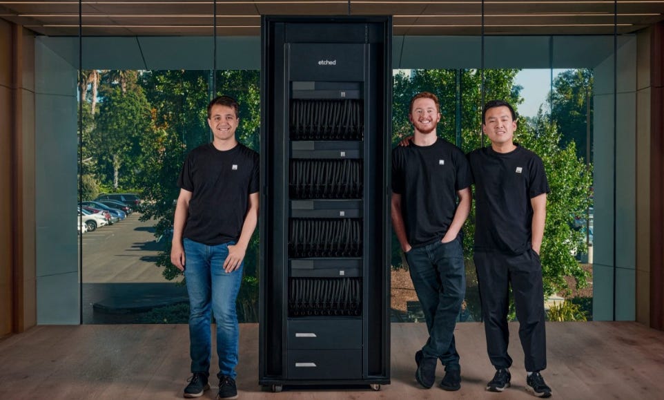
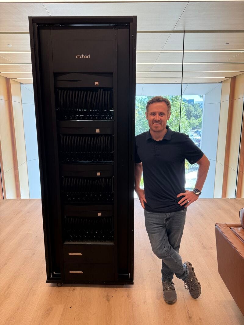
Now Etched has announced they are coming out of stealth with an $500 Million raise (total $800 Million). They built their first racks after a successful A0 tapeout, with $1B+ in customer contracts.


I don’t know how you come out of stealth when we’ve known about your company for 3.5 years but there you have it. Nor do I understand how you call yourself an Nvidia competitor, but that’s the world of dramatics and AI hardware we are currently in, in 2026. They had already come out of stealth in 2023.
Nvidia’s marketshare is actually way bigger in 2026 than it was in 2023 and while AMD and other impress, there’s room for many more as the demand for compute has been surging ahead. Inference is sort of a big deal. The Groq Nvidia deal was big enough.

Strong Engineering and Taiwan Backing
Etched says they have built a team of 400+ engineers from NVIDIA, TPUs, Broadcom, SK Hynix, TSMC, & more.
That their backed by Jane Street, HRT, Two Sigma, and Jump, with strategic investment from VentureTech Alliance. They have deepened their partnership with TSMC among others.
The Series B was led by Stripes, with participation from Ribbit Capital, Radical Ventures, Positive Sum, Primary, & Argo.

What we Know
Their inference systems are built to push the entire pareto curve on frontier models, including many-trillion parameter MoEs, long context, and agentic workloads.
They’ve also co-designed new chips, packages, PCBs, cold plates, interconnects, & more.
They are showcasing two key breakthroughs in mid 2026.
Read their two breakthroughs slowly. And, tell me that’s not impressive for such a young startup?
1. Low Voltage Inference
They introduced this week what they call Low-Voltage Inference (LVI) for high throughput workloads.
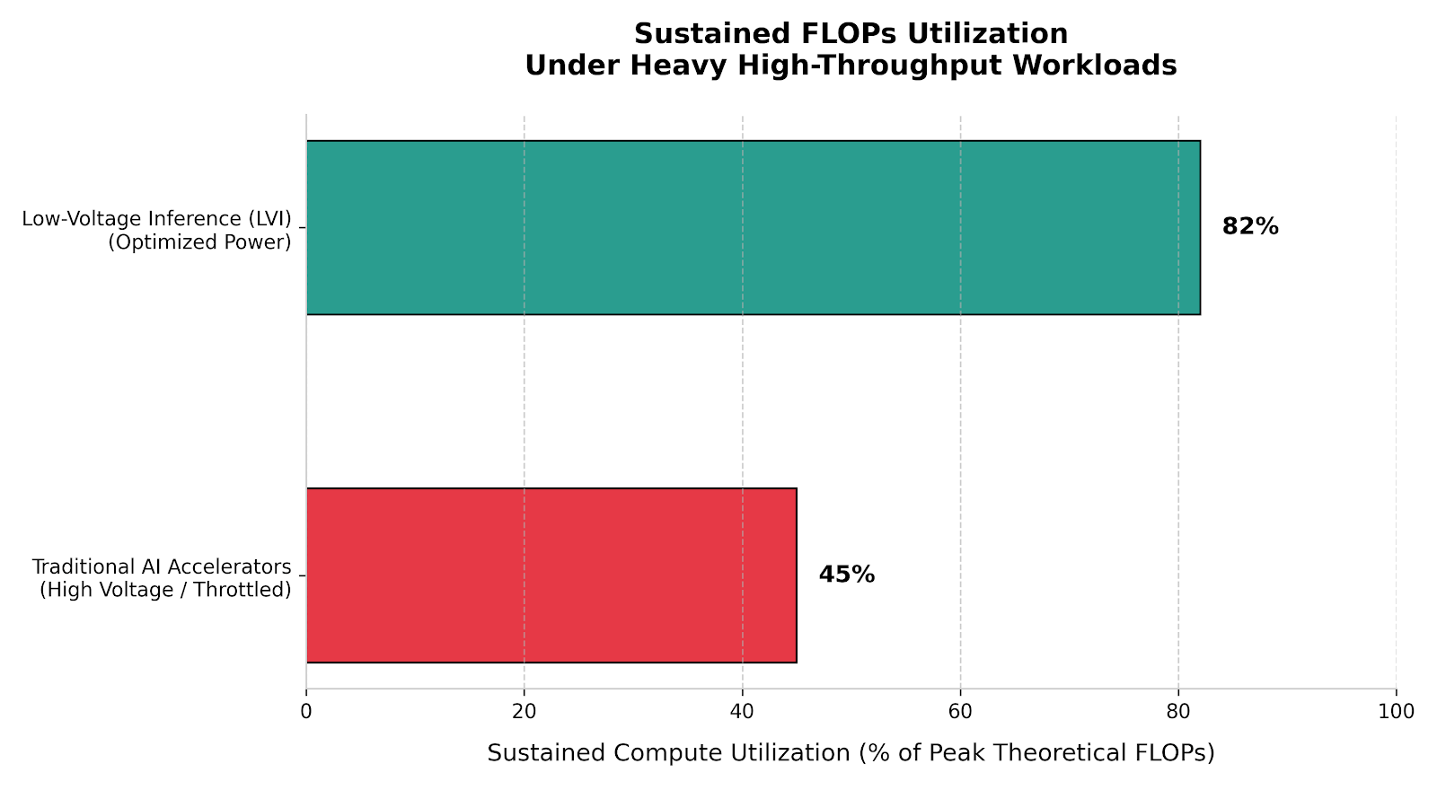
Today, AI chips can't scale FLOPs without thermal throttling.
As FLOPs utilization increases, AI chips draw more power and downregulate clock speed. This often results in sustained inference throughput under half of peak FLOPs.
Chips in other industries solve the power problem by running at lower voltages. Bitcoin miners run at under 3x the voltage of AI chips!
They have designed a new architecture to run our chip’s math blocks at under half the voltage of most AI chips. This enables multiple times the FLOPs density of AI chips today.
They can run trillion parameter sparse MoEs at 80%+ peak FLOPs without thermal throttling.
Running LVI requires co-designing the entire cluster from the transistor to the token: new splittable math arrays, circuit techniques, novel tiling and scheduling algorithms, power delivery networks, VRM architectures, advanced packaging, cold plate designs, and more.

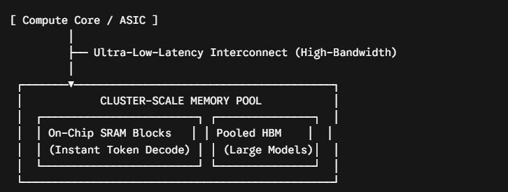
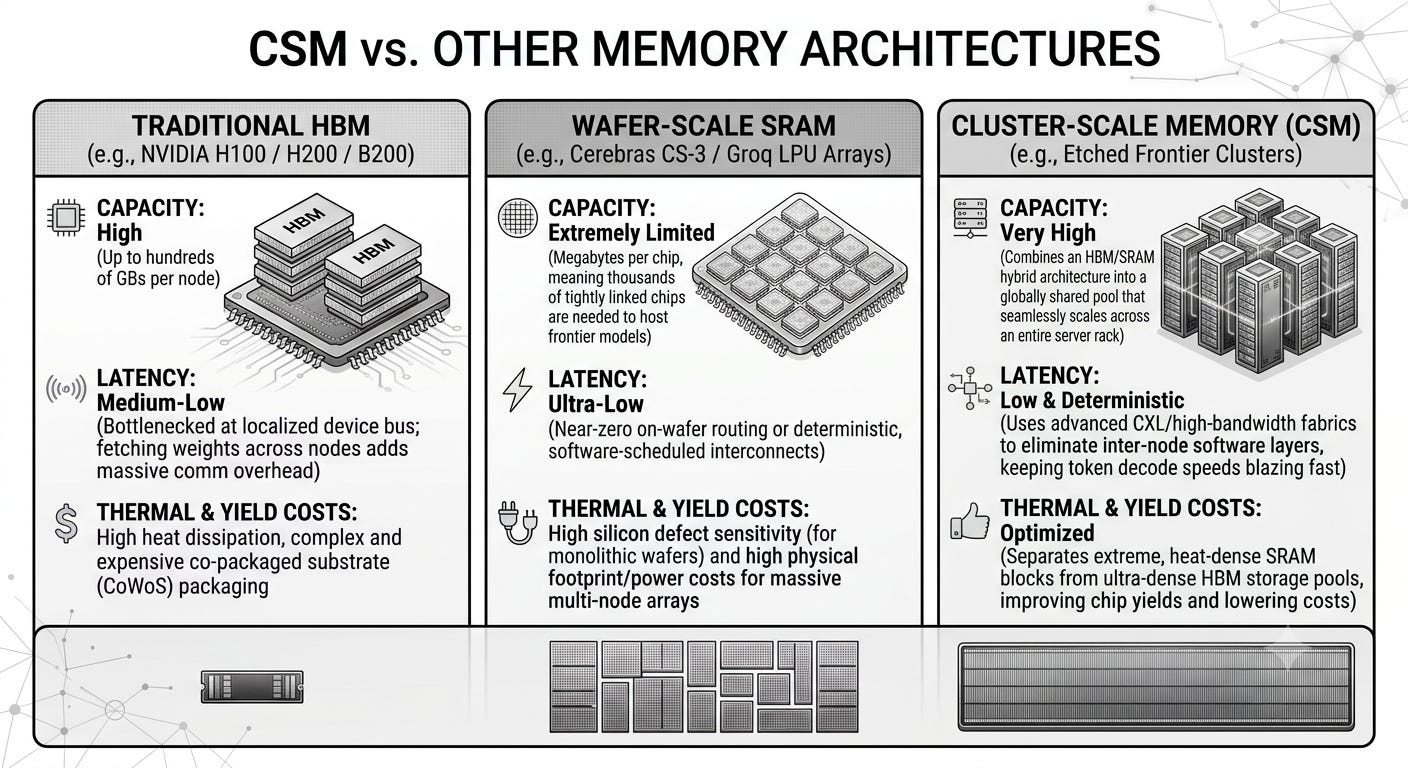
2. Cluster-Scale Memory
Introducing Cluster-Scale Memory (CSM) for low latency workloads.
Today's AI chips using HBM can’t achieve SRAM-level decode speeds due to memory subsystem and interconnect bottlenecks. SRAM-only chips have lower FLOPs density and memory capacity, sacrificing throughput.
You’re forced to make a tradeoff: serve at much slower speeds, or run at low batch sizes and suffer from higher costs.
When running large MoE models, token routing across experts requires sending data through a deep memory hierarchy and a networking switch to reach a destination expert.
Each memory layer inherently adds latency; thus, the best layer is no layer.
They have designed a new architecture that creates a shared low-latency memory pool across the entire scale-up domain.
They use a proprietary ultra-low-latency, high-bandwidth interconnect to enable dramatically faster memory access across chips.
Their HBM/SRAM hybrid design solves both memory capacity and mem2mem latency, enabling high throughput and interactivity simultaneously.
They claim CSM improves latency and avoids today's cost, reliability, yield, thermal, and compute tradeoffs of SRAM-only chips, 3D DRAM chips, or optics.

Latest Details
The company also announced a total of $800M raised across multiple unannounced financing rounds, the latest being $500 million in financing at a $5 billion post-money valuation in December.
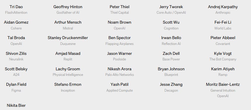
Some of the Angel investors are looking interesting: where backers include VentureTech Alliance, Peter Thiel, Jane Street, Two Sigma, Stripes, Andrej Karpathy, Geoffrey Hinton, and Fei-Fei Li.
The startup says they are scaling production as fast as possible. And have built a 2MW datacenter in their office and opened a Taiwan factory for 24/7 engineering.
It’s the right time to launch their product. Etched first racks ship this summer, targeting frontier models such as many-trillion-parameter mixture-of-experts (MoE) systems, long context, and agentic workloads.
TLDR: Low-Voltage Inference runs its chip’s math blocks at under half the voltage of most AI chips, promising multiple times the FLOPs density.
Cluster-Scale Memory creates a shared low-latency memory pool across chips, using a proprietary interconnect and an HBM/SRAM hybrid design to lift both throughput and speed.
How is their backlog? Not terrible. $1 Billion in Signed Contracts: Etched claims to have secured over $1 billion in sales commitments for its upcoming hardware.
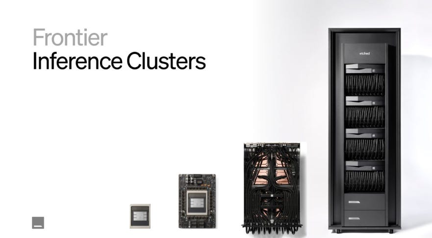
This is a new startup and all somewhat preliminary. Basically Etched is currently in the process of testing that first product with customers. It calls these systems “frontier inference clusters,” (FIC) bundles that include the chips along with custom-designed racks and software, all built to help frontier models run inference faster, more cheaply, and with better power efficiency than rivals.
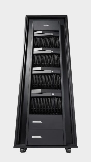
Full stack? Besides creating custom chips, Etched designs its entire server rack — the circuit boards, plates for cooling the chips, networking connections and more. Etched is the only chip startup to have done this, according to Wachen.
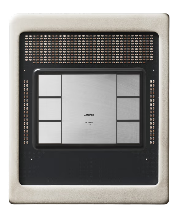
“Etched’s chip, called Sohu, is an ASIC (application-specific integrated circuit) — a chip tailored for a particular application — made for running transformers.”
The Framing
The backing is highly strategic, including massive quantitative trading firms like Jane Street (which has over $100M in them), Hudson River Trading, Two Sigma, and Peter Thiel. Crucially, VentureTech Alliance (in San Jose where they are also based)—a VC firm with deep, strategic ties to TSMC—is on the cap table. The Jane Street and Thiel connections are interesting.
The boys are a little older, the team is a lot bigger and their product looks impressive. Early customer tests show us achieving SOTA throughput, latency, and power efficiency on inference workloads. They have compressed about a decade into two years of work.
Etched is betting on a single architecture in a market dominated by NVIDIA, whose general-purpose chips serve every workload.
The OShaughnessy Interview
Topics:
Why they built an entire rack and not just a chip
The two technical bets behind their architecture no one else has tried
How two founders in their twenties recruited industry legends
The night they nearly ran out of money
Why whoever produces the most tokens wins

0:00 Intro
1:00 Why Nobody Believed Etched Would Work
14:06 Why Inference Is the Bottleneck
22:27 Gavin and Rob’s Origin Stories
33:24 Taking Huge Risks to Move Faster
49:43 Kernels, Compilers, and the AI Stack
1:02:08 Raising $100M to Survive
1:16:00 The Future of Models, Agents, and Intelligence
The Bloomberg Tech Interview
High Profile Angel Investors
Geoffrey Hinton
Peter Thiel
Jerry Tworek
Andrej Karpathy
Shivon Zilis, and more.
“Etched’s chips are unique in that they only run a single type of model: Transformers.” - TechCrunch
Mysterious Jane Street Connection
Jane Street Group is a massive, ultra-private proprietary ("prop") trading firm and market maker. Founded in 2000, they essentially act as a giant middleman in the global financial markets. They are currently experiencing an unprecedented run of success. To put it in perspective, Jane Street generated a jaw-dropping $39.6 billion in net trading revenue. Jane Street has quietly capitalized on the artificial intelligence boom through savvy private market investments. Most notably, they hold a significant early equity stake in Anthropic.
What you have to understand is Jane Street is incredibly well connected. Jane Street has increasingly close, strategic proximity to Taiwan Semiconductor Manufacturing Company (TSMC). In their recent deep-tech deals, Jane Street invested alongside VentureTech Alliance, a venture fund with deep strategic ties directly into TSMC's emerging-businesses orbit.
Jane Street led a previously unannounced funding round, according to Etched co-founder and president Robert Wachen, and has invested additional funds since then. The trading firm has invested a total of more than $100 million in Etched, according to people familiar with the matter.
How Etched Started
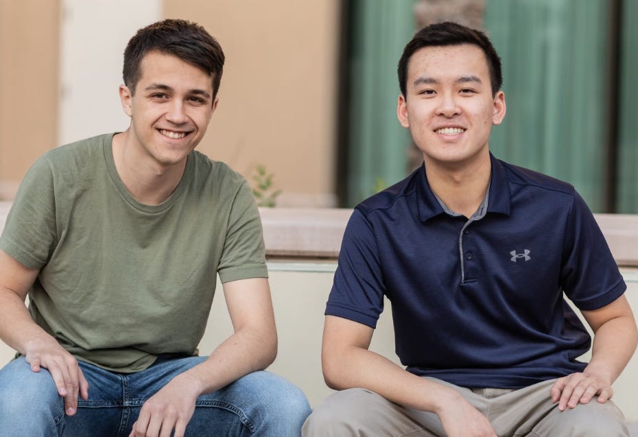
Uberti and Chris Zhu started to work on a chip company after Uberti did a summer internship working on compliers. That put him in contact with the low-level hardware ideas that led to Etched. The pair dropped out of Harvard in 2022, and added Uberti’s college roommate, Wachen.
Back in 2023 the world just wasn’t ready for Etched. Remember back in 2023, they struggled to get investors interested — even with a 30-page memo arguing that AI would eventually need specialized chips, not just general-purpose GPUs. Every major investor they pitched passed. The company was reportedly operating month-to-month, close to running out of cash, in those early days.
Fast forward to 2026 Inference has become a hot topic.

“We went from chip architecture on a napkin to working silicon in TWO years” - Ben Zhou-Chen, Etched.
Status in Mid 2026
Etched is currently in the process of testing that first product with customers.
Their A0 silicon came back from TSMC, manufactured on the N4P (4-nanometer) process, and they achieved first-pass success. They are currently testing and validating the hardware. They say they will have more updates later this Summer.
Will Sohu make tokens cheaper, faster, and less power-hungry than general GPUs? Time will tell. Is Inference the bottleneck? There’s a lot of chip startups now working on this.
Quotes:
Here are some of the quotes I came across about Etched, their team and related topics on what they are building:
“In under four years, Etched has grown into one of the most formidable AI infrastructure teams in the world: 400+ people, including leaders and engineers from Nvidia, Google’s TPU team, Broadcom, SK Hynix, TSMC, top HFT firms, and more.” - Brian Schechter
“We're not doing this just to make a $100B company. We believe inference will become the biggest market of all time, and we want to power a majority of it." - Robert Wachen, Etched
“Etched co-founder/CEO Gavin Uberti is ~24 years old, remarkable
Most chip startup founders are industry veterans
Cerebras's Feldman was AMD VP
Groq's Ross started TPU project at Google
Tenstorrent's Bajic was AMD Director then they got Jim Keller (Intel SVP)
SambaNova's Liang was Oracle SVP
Etched's Uberti in comparison is a recent Harvard dropout. He did work at 3 startups that all got acquired (Xnor, Coursedog, OctoAI)” - Robert Yang. - Source.
“For some intuition on CSM, Cerebras made everyone understand that if you can pool SRAM together on a big wafer you are going to go very fast. Etched can pool the SRAM without needing to keep the dies attached. This means they can push from 8x to 128x to 1000x+ chips all working together in ultra low-latency scale up domains, and then at the same time they can use LVI to pack the die with tons of flops for throughput.” - Orian Leitersdorf - Source.
“(I) Met Gavin at Harvard at a Prod meetup in '24 when they had just raised $500k. going from that to shipping a whole chip and a data center in just 2 years is insane. generational velocity. a totally different league.” - Dev Shah - Source.
“I’ve been watching the (absolutely insane) team at Etched build for years and while this launch is an amazing moment in time snapshot, I believe the market will be amazed at their pace and slope from here.” - Patrick OShaughnessy
“It was abundantly clear that he's (Gavin) a true outlier talent, and talent magnet, and we made Earthshot's largest initial investment up to that point.” - Matt Logan - Source.

Low Voltage Inference
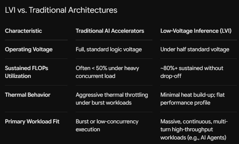
By flattening the thermal curve at the transistor level, LVI maintains a steady, efficient energy state, allowing the chip to consistently extract over 80% of its peak hardware potential without ever needing to pull the emergency brake.
Cluster-Scale Memory (CSM)
In traditional setups, processing units (like GPUs or custom ASICs) are bottlenecked during token generation (the decode phase) because they constantly have to fetch data across deep, fragmented memory layers. CSM addresses this by rethinking physical memory layout at a systemic scale.
Cluster-Scale Memory (CSM) represents a major hardware paradigm shift designed to smash the "memory wall" in high-performance data centers.
The core innovation typically relies on an HBM/SRAM hybrid approach bound together by a proprietary or open-standard (like advanced CXL 3.0 fabrics) ultra-low-latency interconnect.
SRAM (Static Random-Access Memory): Blazing fast but low capacity and highly expensive. CSM utilizes it selectively for extreme throughput during high-interactivity phases.
HBM (High Bandwidth Memory): Dense and high capacity, handling trillion-parameter sparse architectures (like MoEs) or massive KV caches without forcing data out to standard system DRAM.
By unifying these into a deterministic, shared cluster pool, any single chip can access the memory footprint of neighboring chips almost as fast as its own local cache.
Traditional HBM
(e.g., NVIDIA H100 / H200 / B200)
Capacity: High (Up to hundreds of GBs per node)
Latency: Medium-Low (Bottlenecked at the device bus)
Thermal & Yield Costs: High heat dissipation, expensive packaging
Wafer-Scale SRAM
(e.g., Cerebras CS-3 / Groq LPU Arrays)
Capacity: Extremely Limited (Megabytes to low Gigabytes)
Latency: Ultra-Low (Near-zero on-wafer routing)
Thermal & Yield Costs: High silicon defect sensitivity
Cluster-Scale Memory (CSM)
(e.g., Etched Frontier Clusters)
Capacity: Very High (Shared pool scales across the cluster)
Latency: Low & Deterministic (Eliminates inter-node software layers)
Thermal & Yield Costs: Optimized (Separates extreme SRAM blocks from dense storage)
Frontier Inference Clusters
The Transformer-Inference hardware.
Instead of just selling individual chips, Etched is delivering fully integrated, rack-scale hardware systems designed from the ground up specifically to run the world's largest Transformer models—such as multi-trillion parameter Mixture-of-Experts (MoEs), long-context windows, and autonomous agentic workflows.
The Transformer-Only Bet:
The cluster is built around Etched's custom Sohu chip (manufactured on TSMC's N4P process). Unlike a general-purpose GPU, Sohu hardcodes the core algorithms of Transformer attention directly into physical silicon circuits. It cannot run non-transformer architectures (like convolutions or diffusion networks), but by ditching general programmability, it eliminates massive software overhead and achieves unrivaled throughput for LLMs.

This is a new AI startup who are co-designing chips, racks, software, and advanced manufacturing methods for frontier models.
The company promises best-in-class throughput, latency, cost, and power efficiency for both prefill and decode workloads, and they have first silicon proof to back up their claims.
Sohu vs. Nvidia
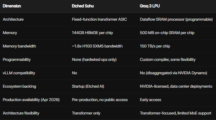
Etched AI’s Sohu is a transformer-only ASIC designed specifically for autoregressive LLM inference. It therefore has a bunch of limitations. But what it’s good at, it’s really good at.
An Inference Rack Solution
Rather than selling standalone ASICs (Application-Specific Integrated Circuits) to be slotted into existing third-party infrastructure, Etched is delivering rack-scale hardware.
Early Angel Investor List
I might be missing a few but these are the ones I found:
TSMC, Jane Street, Hudson River Trading, Jump Trading, Two Sigma, Stripes, Ribbit, Primary, Positive Sum, Peter Thiel, Stanley Druckenmiller, Geoffrey Hinton, Fei-Fei Li, Andrej Karpathy, Arthur Mensch, Tim Rocktäschel, Dean Leitersdorf, Kyle Vogt, Dylan Field, Jesse Zhang, Tri Dao, Scott Wu, Bryan Johnson, Zach Dell, David Baszucki, Jason Citron, and many more.
Additional Links:
Teleology & Founders. The Etched Story.
AI Chip Startup Etched Lures Jane Street, TSMC-Linked VC as Investors
Invest Like Best Interview: YouTube - “The Two Harvard Dropouts Who raised $800M to take on NVIDIA”
Bloomberg Tech Interview June 29th, 2026.
Sohu vs. Nvidia blog.
From San Jose to Taipei
Anyways guys I hope you enjoyed the summary. Looks like they are on the right track. The company has established a vertically integrated footprint, including an NPI prototyping lab in San Jose and a dedicated manufacturing facility in Taiwan.
Cheers,
Mike